Nano Paste
Single Crystal Nano Conductive Pastes and Inks

Metallization paradigm shift
Our Nano Pastes Technology
Low Temperature Curing Pastes for HJT and Perovskite


Our Nano Paste Technology
Low Temp Curing Paste for HJT


Addressing Big Problems in Mega Markets
Nanoparticles
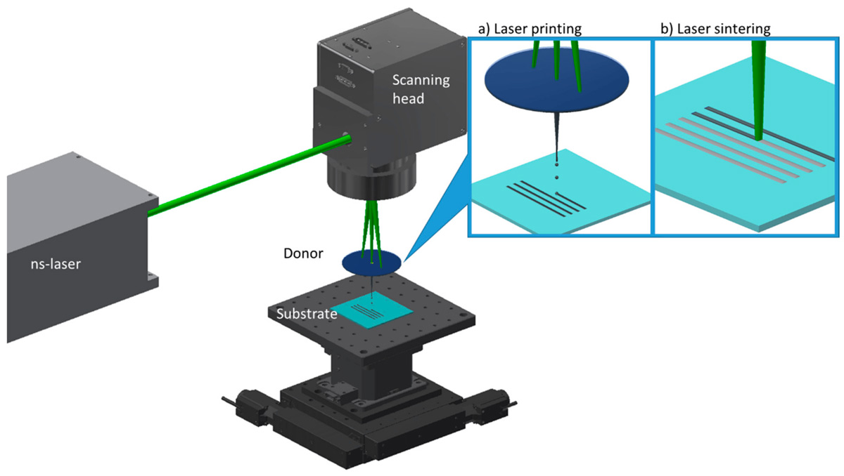
Industrial-scale manufacturing
(high throughput) capabilities optimized for multiple patterning technologies.
pastes for solar metallization
Low temperature, high conductivity pastes lowering HJT and Perovskite $/W, multiple types of metal nanoparticles.
ink applications
Suitable for various mass production applications in additive digital printing
processes such as printed circuit boards, automotive and flexible, customized electronics for the printed electronics field.
Our market focus is solar
In the heart of a perfect storm market with
exponential growth exceeding 30% CAGR,
we solve the bottleneck of metallization,
and pioneering Nano-Paste solutions that
drive the industry’s beyond it’s roadmap.
About Patterning
We’re at the forefront of innovation in nanoparticle patterning, pioneering high metal-loading conductive inks and pastes. Leading solar metallization, providing specialized pastes of Silver and Copper for advanced solar cells. With a unique logistics advantage offering extended shelf life at room temperature storage, we simplify operations for our customers.
With a scalable manufacturing process backed by proven design and FMEA methodology, we ensure reliability and efficiency every step of the way.
Join us as we redefine possibilities in the world of technology and manufacturing.
Learn More